
CCDs, like valves before them, convert optical images into electronic images that can be stored electronically. CCDs were invented in 1969 by Willard Boyle and George Smith at the AT&T Bell Labs in New Jersey, USA, for which they shared the 2009 Physics Nobel Prize.
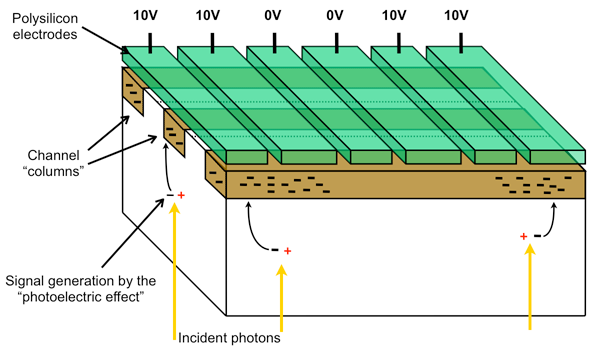
Figure 1: Schematic of a small part of a CCD, illustrating photons being converted into electrons via the photoelectric effect and being attracted to the potential wells under electrodes with positive voltage applied. Copyright Oxford University Press. (Reproduced with permission of the publisher on a free-to-view basis only and not included under the website's Creative Commons license.)
When photons interact with the silicon inside CCDs, they are converted into electrons via the photoelectric effect (see Figure 1). Applying a positive voltage to some parts of the silicon via a number of electrodes causes different electric potential wells to form. The newly converted electrons are attracted to the nearest potential well, where they coalesce to form charge packets.
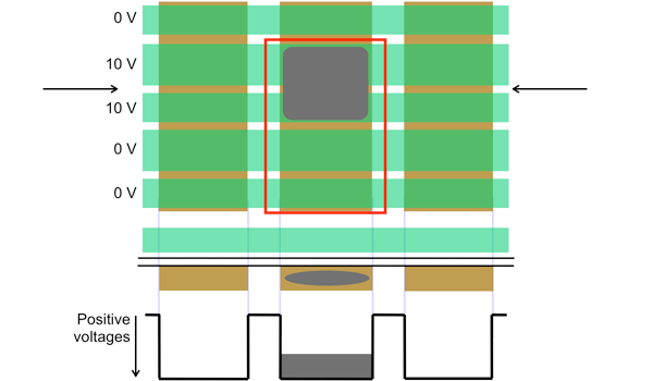
Figure 2: Top: Schematic of a small part of a CCD from above, illustrating a charge packet (grey) sitting under two electrodes applied with a positive voltage and the other two electrodes with no voltage applied making up a pixel (outlined in red). Bottom: Cross-section through a small part of a CCD, starting with the electrode (solid green block). Underneath are "buried (potential) channels" (brown blocks), created in the silicon by applying positive voltages to the electrode, with a charge packet (grey) sitting in the middle buried channel. Below these, the potential wells of the buried channels are illustrated, with a charge packet sitting in the bottom of one of the potential wells. Copyright Oxford University Press. (Reproduced with permission of the publisher on a free-to-view basis only and not included under the website's Creative Commons license.)
Different charge packets are separated by regions of silicon without a voltage applied to it. The region containing a charge packet and its separation to the next charge packet is called a pixel or picture (pix) element (el). A pixel is the smallest component of a digital image (see Figure 2). These charge packets can be moved from pixel to pixel (in order to read them out) by changing the voltage applied to the electrodes in the correct sequence.
Next: The Gaia CCD challenge
Page last updated: 05 June 2014